A history of NVIDIA Streaming Multiprocessor (part 2)
A few weeks ago, I stumbled upon this awesome blog post[1] by Fabien Sanglard. It goes into great detail on the evolution of NVIDIA's streaming multiprocessors and the design choices behind the different architectures throughout the years.
The article was published on May 2, 2020, when the last released architecture was Turing (2018), and Ampere was just weeks from release. Since then, NVIDIA has released four different architectures, LLMs exploded in popularity, and the demand for massively parallel processors has risen to an all-time high.
In this blog post, we are going to visit the newer SM architectures and try to answer a few thoughts Fabien left by the end of his article:
What will be interesting is to see how Nvidia keeps on evolving now that their dies have three types of cores serving different purposes. Will we see dies entirely made of Tensor cores or RT cores? I am curious to find out.
Visited in this blog post:
| Year | Arch | Series | Die | Process | Consumer GPU | Data Center GPU |
|---|---|---|---|---|---|---|
| 2020 | Ampere | GeForce RTX 30 series | GA102 | 8 nm | RTX 3090 Ti | A100 |
| 2022 | Ada Lovelace | GeForce RTX 40 series | AD102 | 5 nm | GeForce RTX 4090 | RTX 6000 Ada Generation |
| 2022 | Hopper | - | GH100 | 5 nm | - | H100 | H200 |
| 2024 | Blackwell | GeForce RTX 50 series | GB202 | 5 nm | RTX 5090 | B200 | B300 |
Ampere
In 2020, Nvidia released the Ampere architecture. This newer generation built upon features introduced in Volta and Turing, delivering significantly faster performance and ultimately cementing that raytracing and tensor cores are here to stay.
One of the biggest improvements in the GA10X SM was its FP32 throughput[2]. Unlike the TU102 SM, which had two primary datapaths, with only one being able to process FP32 operations (the other was limited to integer operations), Ampere’s newer SM includes FP32 processing on both datapaths. This meant that effectively, it executes double the FP32 rate of the Turing SM per clock.

GA10x Streaming Multiprocessor (SM)
As expected, the new SM also introduced second-generation Ray tracing cores. It allowed RT Cores and graphic/compute workloads to be processed concurrently in each SM, doubling ray/triangle intersection performance compared to the first generation[2].
Improvements also came to the Tensor Core, now in its third generation. By introducing Fine-Grained Structured Sparsity[3], it doubled the effective throughput[4]. It is worth noting that Ampere has only half the number of Tensor Cores per SM compared with Turing, though they are way more powerful.
Ada Lovelace
In 2022, Nvidia released a new architecture named after the legendary mathematician Ada Lovelace, considered to be the first computer programmer. While improvements in the silicon manufacturing process have slowed, Ada was “the largest generational performance upgrade in the history of NVIDIA”[5], marking the tipping point where ray tracing and neural graphics became mainstream.
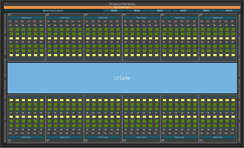
AD102 GPU powered by 144 AD10x SMs
Compared to its predecessor, the new AD10x SM doesn't seem all that different, so how could it be that much of an upgrade?
One of the most important factors was the improved manufacturing process. While Ampere GPUs were developed using Samsung's 8N process, Ada used TSMC's 4N process. This allowed the new AD102 GPU to contain 70% more CUDA Cores than the prior generation GA102 GPU, while operating at higher frequencies. Not only that, but it also had the highest performance per watt [5].
As of every new generation, Ray Tracing and Tensor cores also received upgrades.
Ada’s Third-Generation RT Core offered 2x faster ray-triangle intersection throughput over prior generation Ampere GPUs and it also included two new hardware units: an Opacity Micromap Engine and the Displaced Micro-Mesh Engine[6].
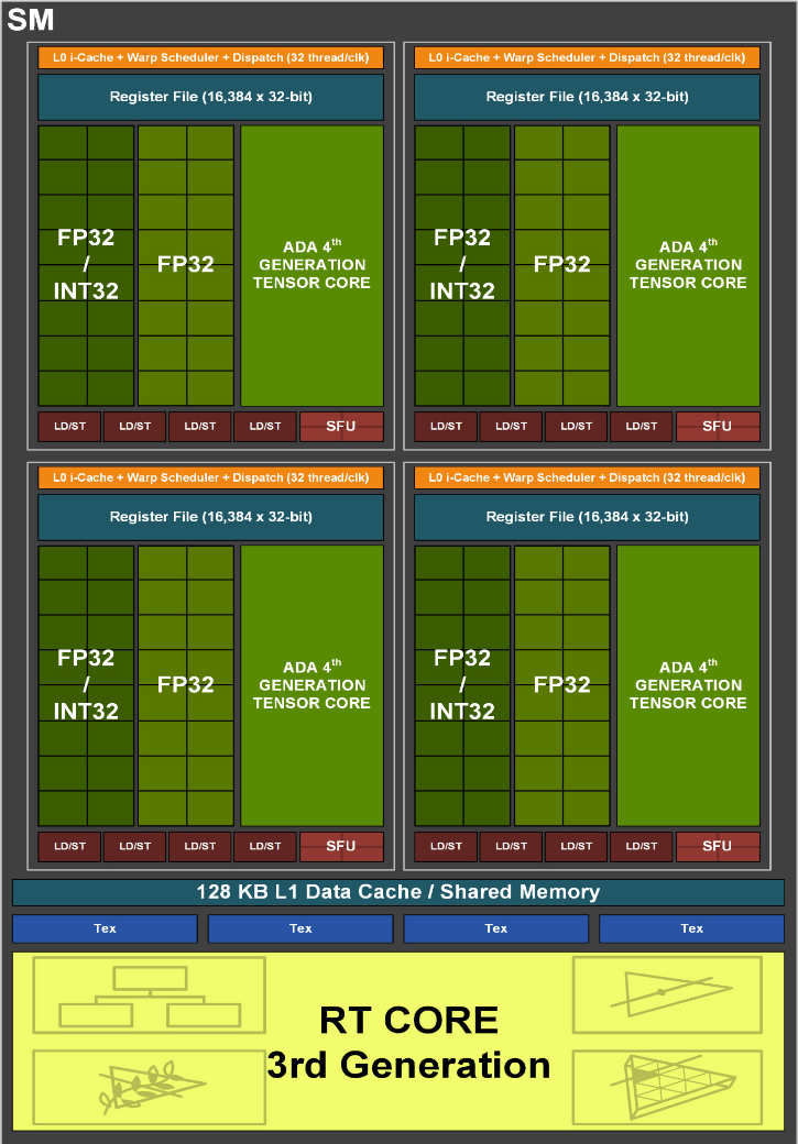
AD10x Streaming Multiprocessor (SM)
Ada's Fourth-Generation Tensor Core delivered more than double the FP16, BF16, TF32, INT8, and INT4 Tensor TFLOPS compared to previous generation tensor cores and also included the Hopper FP8 Transformer Engine, which we'll visit later.
Hopper
While Ada was mainly aimed at consumer GPUs, in the same year Nvidia announced the Hopper architecture alongside the behemoth H100 Tensor Core GPU, packed with 80 billion transistors[8]. This was also the year ChatGPT launched, bringing AI into the mainstream and making the H100 the most sought-after chip on the planet.
The H100 was the first GPU to support PCIe Gen5 and the first to utilize HBM3, enabling 3TB/s of memory bandwidth. Twenty H100 GPUs can sustain the equivalent of the entire world's internet traffic[9].
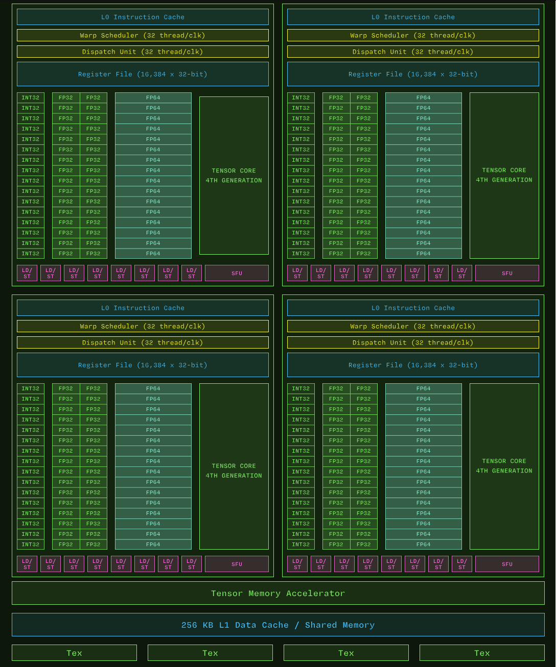
GH100 SM. Image from Modal's GPU Glossary (check it out, it's great!).
A major new feature introduced was the Tensor Memory Accelerator (TMA), which performs asynchronous memory copy between global and shared memory, bypassing register files entirely. You can learn more about it here and here.
The H100 also extended the CUDA programming model. It Introduced an optional level of hierarchy called Thread Block Clusters that are made up of thread blocks. Thread blocks in a cluster are guaranteed to be co-scheduled on a GPU Processing Cluster (GPC) and all their threads have access to the Distributed Shared Memory, enabling more efficient data sharing and communication across blocks.
It also features a Transformer Engine, a custom Hopper Tensor Core technology designed specifically to accelerate the training and inference of transformer-based AI models. These Tensor Cores can apply mixed FP8 and FP16 formats to dramatically accelerate AI calculations for transformers.
Other notable improvements include the addition of DPX instructions, which accelerate dynamic programming algorithms by up to 7×, as well as enhancements to NVLink, NVSwitch, and the NVLink Switch System.
One fun fact that I found while researching this topic is that the H100 is apparently going to outer space. Extraterrestrial data centers. What a time to be alive.
Blackwell
Finally, the (current) state-of-the-art. Released in 2024, when the AI boom was in full swing, Blackwell represents NVIDIA's most aggressive push toward AI-optimized hardware yet. We'll be spending a bit more time on this architecture, since it's the most powerful ever built and since I personally own an RTX 5060 and want to learn how to push this hardware to its limit.
For this generation, NVIDIA decided to not develop two separate named architectures for different types of consumers. Instead, the NVIDIA Blackwell architecture family includes both RTX Blackwell and Blackwell datacenter-class GPUs, each with with distinctive flagship chips.
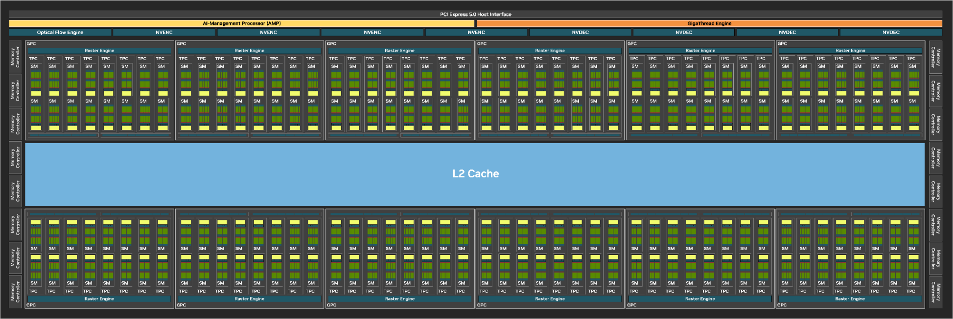
GB202 GPU block diagram (full chip) with 192 SMs. It's huge.
Let's first explore the GB202 chip. It is the flagship of the the GeForce RTX 50-series and it powers the GeForce RTX 5090 graphics card.
When looking at the Blackwell SM, the first thing we notice is that each CUDA core cluster now has 32 ALUs capable of either 32-bit floating point or integer operations, returning to the Pascal-style unified FP32/INT32 datapath instead of separate cores as in Ada Lovelace.
According to the whitepaper[10], Ada’s SM was designed and optimized for standard shaders while Blackwell SM was designed and optimized for neural shaders.
As a result, both RT and Tensor Cores received upgrades.
Blackwell's 5th-generation Tensor Cores now add support for FP4 and FP6 operations, alongside the new second-generation FP8 Transformer Engine, similar to Blackwell datacenter-class GPUs.
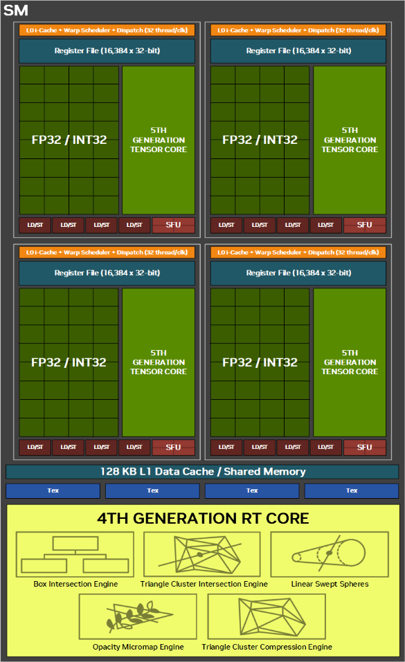
The Blackwell Streaming Multiprocessor (SM)
The Fourth-Generation RT Cores in the Blackwell architecture provides double the throughput for Ray-Triangle Intersection Testing over Ada. They now have a new dedicated unit known as Triangle Cluster Intersection Engine which accelerates ray tracing of Mega Geometry, a new RTX technology.
RTX Blackwell also introduced brand new GDDR7 Memory, achieving up to 1.792 TB/sec peak memory bandwidth.
It also includes an AI Management Processor (AMP), which is a fully programmable context scheduler designed to offload scheduling of GPU contexts from the CPU. This allows smoother frame rates in games, and better multitasking in Windows because the CPU is less burdened
For datacenter/AI workloads, NVIDIA has released the B200 , B300 and the GB200 Grace-Blackwell Superchip as replacements to Hopper's H100 and H200.
The future
Announced at Computex 2024 in Taipei by CEO Jensen Huang, the next architecture, codenamed Rubin (as in Vera Rubin) will feature a GPU named Rubin and a CPU named Vera, both manufactured by TSMC using a 3 nm process and equipped with HBM4 memory. Whether it will reach the gaming consumer market remains unknown. Mass production is expected to begin in late 2025, with availability projected for 2026.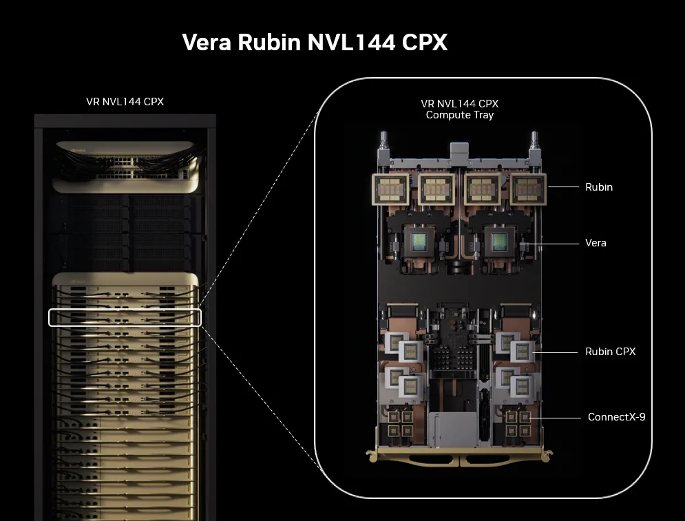
NVIDIA Vera Rubin NVL144 CPX rack and tray featuring Rubin Context GPUs (Rubin CPX), Rubin GPUs, and Vera CPUs
At GTC 2025, Jensen Huang announced the Feynman microarchitecture, expected to arrive in 2028.
Conclusion
When Fabien wrote his original post, he wondered whether we'd see GPUs composed entirely of Tensor or RT cores.
What will be interesting is to see how Nvidia keeps on evolving now that their dies have three types of cores serving different purposes. Will we see dies entirely made of Tensor cores or RT cores? I am curious to find out.
Five years later, the answer seems to be: not quite. While we haven’t seen GPUs composed entirely of Tensor or RT cores, what we have witnessed instead is a clear and deliberate shift in focus toward accelerating AI workloads.
I wonder what new forms of specialized AI capabilities the next generations of SMs will bring, and whether at some point the Streaming Multiprocessor itself will evolve into something entirely new.
These architectural changes also raise a broader question about NVIDIA itself. I'm curious to see how the company continues to evolve as an AI-first company, and how this strategic focus will shape the direction of its future architectures and technologies.
References
- A history of NVidia Stream Multiprocessor
- NVIDIA AMPERE GA102 GPU ARCHITECTURE
- How Sparsity Adds Umph to AI Inference
- NVIDIA A100 Tensor Core GPU Architecture
- NVIDIA ADA GPU ARCHITECTURE
- NVIDIA Micro-Mesh
- Improve Shader Performance and In-Game Frame Rates with Shader Execution Reordering
- NVIDIA H100 Tensor Core GPU Architecture
- NVIDIA Announces Hopper Architecture, the Next Generation of Accelerated Computing
- NVIDIA RTX BLACKWELL GPU ARCHITECTURE